sábado, 24 de julio de 2010

PZE Energy Harvester


As wireless sensor nodes become smaller, their energy supply is a limiting factor for further miniaturization as integration density is limited by the space requirements of the energy storage system. MEMS based energy harvesters, such as the one shown in this example, are becoming a key enabler for further miniaturization and deployment of energy autonomous sensor nodes.

Vibration harvesting taps into energy present in moving structures. Several physical effects can be employed to transform mechanical to electrical energy. Piezoelectric, electrostatic or electrodynamic effects are the most common approaches. In this example we show a piezoelectric vibrational energy harvester, similar to the devices shown in Figure 1, fabricated from silicon by a combination of wet and dry etching techniques. This device is designed to be integrated into a energy harvesting module together with a power transfer circuit, a storage element and a resistive load.

Figure 1: Various piezoelectric energy harvesters packaged between two glass substrates. Image courtesy of Holst Centre / IMEC The Netherlands.


Modeling:

A finite element model created in CoventorWare's Designer, comprising a cantilever beam, seismic mass, piezoelectric layer and electrode layers is shown in Figure 2. The cantilever and beam is meshed with 27-node hexahedral elements, the piezo layer with 20-node piezoelectric hexahedral elements. Note that bond pads and conductive path are considered to have a negligible effect on the response and thus omitted in this model. Literature values for the mechanical properties of silicon and the piezoelectric properties of the Aluminium Nitride layer are also used.


Figure 2: CoventorWare Finite element model of a piezoelectric energy harvester showing the mass, cantilever beam, anchor point and PZE layers.

Simulation

CoventorWare's Analyzer modules can be used to simulate the harvester. When a load resistor is directly connected to the harvester, the dissipated power varies over time according to the changing output voltage of the harvester. Of particular interest is the value of load resistance where maximum power transfer from the harvester occurs. To determine the variation of power disspated with load resistance, mechanical boundary conditions were imposed at the anchor point and the harmonic response under a 0.25g load acceleration simulated. The device operates under atmospheric pressure and experiences drag forces under motion. This distributed effect was included in the model by incorporation of Rayleigh (material) damping. The related coefficients were adjusted in order to correctly reflect the quality factor of actual devices operating at atmospheric pressure.

Results

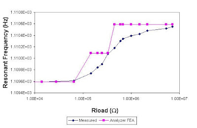
Figure 3 and Figure 4 compare measured and simulated values for average power dissipated and resonant frequency with load resistance, respectively. The measured data accuracy is estimated to be 6%. Predicted power dissipation is within about 25% of the nominal measured values, mesh refinement on selected simulations suggest a reduction to 21% is possible. The remaining difference is likely due to slightly high material damping values used for simulation. Figure 5 shows an animation of harmonic displacement magnitude together with the real voltage on the upper electrode.
Figure 3: Comparison of simulated and measured average power dissipated in a load resistor at 0.25 g acceleration. Note the measured point at Rload of 7.1 Mohm is likely erroneous.
Figure 4: Comparison of simulated and measured shift in resonance frequency at 0.25 g acceleration. The step in the simulated data is due to the 0.25 Hz frequency increment of the harmonic analysis


Figure 5: Animation of harmnonic simulation showing displacement (scaled by a factor of 20) and real voltage developed on the upper piezo surface.

Nombre: Lenny D. Ramirez C.
Asignatura: CRF
Dirección: http://www.coventor.com/mems/applications/PZE_Energy_Harvester.html
Ver blogg: http://lennyramirez-crf3.blogspot.com/

Dual Mass Gyroscope


This dual mass gyroscope consists of two perforated proof masses supported by a system of suspension elements. Attached to the ends of each proof mass are interdigitated comb-finger capacitors. The comb capacitors are used for electrostatically driving the proof masses in anti-phase in a mode parallel to the substrate (the x direction). Rotation about the in-plane y-axis induces a Coriolis force, which deflects the proof masses in opposite directions, perpendicular to the substrate. Beneath the plates are deposited metal electrodes that are biased with a DC voltage. The proof mass motion in the z direction, resulting from the rotation of the gyroscope, induces current flow on the electrodes, which is then measured. Figure 1 shows the 3-D model of the gyroscope.

Figure 1: 3D model of the dual mass gyroscope. For clarity, the model has been scaled factor of 2 in the Z direction


Modeling:

In this example, Architect is employed to build a fully parametric, 3-D model of the gyroscope using plates, beams, electrodes and comb-finger elements from the Parameterized Electromechanical (PEM) parts library. Figure 2 shows the Architect schematic of the gyroscope.


Figure 2: Architect schematic of dual mass gyroscope

The perforated proof masses are modeled using components labeled "Rigid Plate". Similarly, the electrodes beneath the proof masses, which sense the proof mass motion, are modeled by components labeled "Electrode". The comb drives on either side of the two proof masses are modeled by "Straight Comb" components. The suspension elements for the proof masses are modeled using a combination of "Box-beam" and "Beam" components. Note that the Architect PEM parts library has a variety of beam-like suspensions structures, and a single "Box-Beam" element could therefore be used instead of using four rectangular "Straight" beams.
Simulation

Figure 3a shows the simulated displacement of the proof mass in the x and z direction over a period of 50ms. Figure 3b shows the first 5ms only. The simulation starts from the steady state, computed with a small signal AC analysis. The excitation voltages applied to the comb-drives vibrates the proof masses in the x direction at a frequency of 16.987 KHz. Angular velocity applied about y direction, after 1ms, induces a Coriolis force that causes proof mass motion in the z direction. This motion is sensed by measuring the difference in capacitance, "Delta Cap" in the output plot, between the two sensing electrodes. After 25ms the rotation rate about the y axis returns to zero, and the output signal decreases to a steady-state value. In this simulation modal (Rayleigh) damping models are used for the beam and velocity damping values used for the plate. The fully coupled electro-mechanical 50ms simulation takes about 1 hr to run on a 2 GHz processor.

Figure 3a: Gyroscope transient simulation showing input rotation about y, sense capacitance "delta cap", (right) mass displacement "x" and "z".


Figure 3b: Gyroscope transient simulation from (a) with response from 0 to 5.0ms.


Figure 4: Animation of transient simulation. For clarity, the fixed electrodes and the comb drives are transparent and the thickness scaled by 2. The displacement in Z is also scaled by a factor of 1,00,000 to allow the movement of the gyroscope to be resolved.


Nombre: Lenny D. Ramirez C.
Asignatura: CRF
Dirección: http://www.coventor.com/mems/applications/Dual_mass_gyroscope.html
Ver blogg: http://lennyramirez-crf3.blogspot.com/

Ring Gyroscope


This Ring Gyroscope is constructed from an outer ring, eight semicircular support springs, drive, sense and control electrodes, see Figure 1. The Gyroscope has two identical elliptically-shaped flexural-modes of that are of equal frequency and separated by a 45 degree angle, see Figure 2. The ring is excited electrostatically into the primary flexural mode, and held at a fixed amplitude. As device is subjected to rotation around its normal axis, Coriolis force causes energy to be transferred from the primary mode to the secondary mode, causing the secondary mode amplitude to increase. This amplitude change is sensed capacitively.


Figure 2: The first and second modes of the gyroscope. (a) first flexural mode, and (b) second flexural mode located 45 degrees apart from the first. Both modes have the same frequency.

Modeling:

Architect can be used to build a fully parametric 3D model of the Gyroscope using beams and electrodes from the Parameterized ElectroMechanical (PEM) parts library. Figure 3 shows the schematic of the Gyroscope. In the schematic, a sub-assembly has been used to represent the eight springs in the gyroscope. This makes it easier to construct and understand the schematic. Figure 3a shows the top level schematic while figure 3b shows the lower level hierarchical element. The semicircular support spring is modeled using a combination of 'Arc beam' and 'Beam' components from the PEM parts library.


Figure 3: Hierarchical Ring Gyroscope schematic in Architect, (a) top level schmatic  and (b) lower level hierarchical elements

Simulation:
Figure 4 shows the frequency response of the Gyroscope, generated via a small signal ac analysis. The frequency at which the Gyroscope has flexural modes is 27.085 KHz. The simulation time for this analysis is ~1 second on a 2 GHz laptop. Figure 5 shows an animation of the flexural mode shape at the resonant frequency, created using Scene3D.

Note that process variations can cause asymmetry in the ring structure which will lead to separation of the modes. Architect can help you understand the separation in resonances with process variation.
Figure 4: Small signal ac analysis result showing the displacement magnitude response at 27087 Hz


Figure 5: Animation showing first flexural mode. For clarity, the displacement is scaled up by a factor of 5000


Nombre: Lenny D. Ramirez C.
Asignatura: CRF
Dirección: http://www.coventor.com/mems/applications/Ring_gyroscope.html
Ver blogg: http://lennyramirez-crf3.blogspot.com/
MEMS Products Available in the Market


Freescale ZSTAR3: the multiple wireless sensing triple-axis reference design

The ZSTAR3 development tool contains one accelerometer transmitter boards and one USB receiver node. A ZSTAR3 system can accommodate upto 16 accelerometer transmitter boards, connected through an RF ZigBee 2.4GHz communication to a single USB node connected to a PC. The accelerometer boards measured acceleration in 3-axes using either a digital or analog sensor. The sensor sensitivity is defined by the selected accelerometer. The USB node is part of the ZSTAR and ZSTAR2 design, reprogrammed with dedicated SW supporting multiple nodes.


STMicroelectronics Unveils MEMS Digital Compass Module

STMicroelectronics (NYSE: STM), the leading supplier of MEMS for consumer and portable applications(1), has integrated a 3-axis digital accelerometer with a 3-axis digital magnetic sensor in a single module. The digital compass module combines high accuracy with small form factor and low power consumption at a competitive cost, meeting the growing market demand for advanced navigation capabilities and emerging smart location-based services. ST's high-performance system-in-package digital compass uses magneto-resistive technology from Honeywell and aims to accelerate the adoption of enhanced electronic compassing in portable consumer applications, including direction finding, map/display orientation, location-based services and pedestrian dead reckoning.


The LSM303DLH geomagnetic module combines magnetic-field and linear-acceleration sensing with an I²C digital interface in a single package, featuring six degrees of freedom (DoF).

The module offers:
- 3-axis acceleration sensor with user-selectable ±2 to ±8g full scale acceleration,
- a 3-axis magnetic sensor with user-selectable full scale (±1.3 to ±8.1 gauss).
The LSM303DLH includes, for each sensing element, an embedded self-test that can be performed before assembly, and smart power functionalities to minimize current consumption.
The module features two separate user-configurable interrupts for inertial wake-up and free-fall.


Epson Toyocom Develops the World's Smallest Single Package 6-Axis Sensor

Epson Toyocom Corporation, the leader in crystal devices, today announced the development of the AH-6100LR, the world's smallest* 6-axis sensor. This low-noise, low-power product comprises a 3-axis QMEMS*1 quartz gyro-sensor and an extremely stable 3-axis accelerometer within a single package.
Samples of the new AH-6100LR will become available in February 2010. Commercial development is scheduled for May 2010.


Colibrys New MEMS Accelerometer for Attitude Heading and Reference Systems (AHRS)

Colibrys (Switzerland) Ltd. has announced today the release of its new MS9005, a ±5g range MEMS accelerometer, to complement its existing family of +/-2g and +/-10g products targeted primarily at AHRS applications.

Current and future developers of AHRS using Colibrys accelerometers will benefit from this new product as an alternative to existing selection of products, which are the traditional Colibrys-MS9002 and MS9010 sensors dedicated to standard AHRS and the latest world's best open-loop RS9010 accelerometer dedicated to mid range requirements.

According to Jean-Michel Stauffer, VP Sales & Marketing at Colibrys, "the MS9005 offers optimal accelerometer performance for applications that operate in medium level vibration and shock environment but where absolute bias and scale factor stability and reduced VRE (Vibration Rectification Error) are valued. Typical examples of AHRS integrating Colibrys accelerometers are airplanes, helicopters and UAV as well as backup systems on large aircrafts and small jets. This new product strengthens Colibrys' position as the world leading supplier of MEMS accelerometers for AHRS applications"

his product benefits from the specialised knowledge and applications experience of Colibrys accelerometers in term of reliability for harsh environments and safety critical applications.


Nombre: Lenny D. Ramirez C.
Asignatura: CRF
Dirección: http://info.coventor.com/mems-products/
Ver blogg: http://lennyramirez-crf3.blogspot.com/

MEMS resonator: Thermo-Elastic Damping and Anchor Loss models


Resonator Design In CoventorWare

One of the design consideration for MEMS Resonators is the Quality Factor (Q). This is the ratio of the total stored energy to the energy dissipated in a single cycle. At a particular oscillation frequency, a higher Q indicates a lower rate of energy dissipation and oscillations die out more slowly.

Numerous physical loss mechanisms contribute to overall Q and can be expressed as:

QGAS

Air Damping: Squeeze film or Stokes
Minimized by operating in a vacuum
Coventor's Solution: Rayleigh Damping Coefficients

QTED

Thermoelastic Damping: As a vibrating body is strained, the temperature changes in proportion to the strain; when temperature gradients occur, heat conduction causes irreversible energy loss
Coventor's Solution: Thermoelastic Damping Option

QANCHOR

Anchor Loss: A fraction of elastic energy propagates into the surrounding support structure
Also referred to as support loss, clamping loss, or attachment loss
Coventor's Solution: QuietBoundary Surface Boundary Condition

QOTHER

Other Loss Mechanisms: Including structural dissipation (crystallographic defects) and surface effects
Coventor's Solution: Rayleigh Damping Coefficients
Thermoelastic Damping
The Thermoelastic Damping can contribute significantly to Q in MEMS resonators operating in vacuum. CoventorWare-ANALYZER's MemMech module calculates the energy lost to heat conduction caused by strain-induced temperature gradients. This direct harmonic analysis simulate in 32-bit mode and requires material properties such as thermal expansion coefficient (TCE Integral Form), thermal conductivity and specific Heat.

Temperature distribution during Thermo-Elastic Damping Simulation


TED Energy Distribution during Thermo-Elastic Damping Simulation


The graph below shows a comparison between a Thermo-Elastic Damping model that has been implemented in CoventorWare-ARCHITECT, Finite Element results from ANALYZER and analytical models.


Losses
Anchor losses result when anchors are stressed as a result of resonator displacement. A fraction of the vibration energy is lost from the resonator though elastic wave propagation into substrate. In MEMS structures we usually assume all elastic energy transferred to the substrate is lost, although the mechanism is not fully understood. Anchor losses can be significant if contributions from other loss mechanisms are negligible. Having a simulation tool provides the ability to investigate optimal anchor placement.
Acoustic waves propagate through the substrate causes energy loss at the anchor


The anchor loss can be calculated by modeling the resonator and a fictitious substrate, these are linked together in the simulation automatically (this avoids overly fine meshes). In addition a so called "QuietBoundary" boundary condition is applied which models elastic waves propagating to infinity in the substrate, eliminates the reflection of the elastic waves impinging on the boundary or excitation origin.

The results can be analyzed by plotting the harmonic displacement to identify the harmonic frequency closest to resonance. The Q factor and Harmonic Energy values can then be determined as can be seen in the result graph below:


Determining the Q factor from anchor loss calculations


Nombre: Lenny D. Ramirez C.
Asignatura: CRF
Dirección: http://info.coventor.com/memsahead/bid/34328/MEMS-resonator-Thermo-Elastic-Damping-and-Anchor-Loss-models
Ver blogg: http://lennyramirez-crf3.blogspot.com/

MEMS BUTTERFLY: Give your ideas wings with MEMS+ 2.0


Nature has inspired many designers to create new products that we use in our every day lives. The butterfly seems to be popular among scientists, see Qualcomm's iMOD display and others have designed gyroscopes.

Similarly, Coventor's product development created a test case inspired by the butterfly to demonstrate the new amazing capabilities of the MEMS model library that will be released in MEMS+ 2.0 in June this year.

The video above gives you a sneak preview of what's going to be possible with our upcoming MEMS+ 2.0 release.

Fastest computation of MEMS structures in Cadence Spectre

The video shows the first Eigenmode of a butterfly made of our new flexible plate components. The butterfly test structure was made of circular, quadrilateral and pie shaped flexible plates. Featuring 92 nodes, it was simulated in only 5 seconds with an AC analysis using Cadence Spectre. Constructing the model in MEMS+ 2.0 Innovator took less then 5min


AC simulation of the movement of butterfly wings using MEMS+ and Cadence Spectre

MEMS+ 2.0 user interface with access to foundry material and process data, 3D graphical interface for model creation and the MEMS model library.


Visualization of the connecting nodes of the 3D model. After creation of the 3D geometry the model can be simulated immediately in Cadence Spectre or UltraSim.


Nombre: Lenny D. Ramirez C.
Asignatura: CRF
Dirección: http://info.coventor.com/memsahead/bid/38416/MEMS-BUTTERFLY-Give-your-ideas-wings-with-MEMS-2-0
Ver blogg: http://lennyramirez-crf3.blogspot.com/

Dispositivos mecánicos ultra pequeños MEMS


Para fijar ideas podemos decir que en el microprocesador de una computadora actual tenemos unos 50 millones de transistores por cm2, lo que implica una dimensión típica de 1 m2 por transistor, con un detalle de los contornos del orden de los 100 nm. Esta miniaturización ha permitido reducir componentes electrónicos voluminosos dando a lugar a equipos portátiles, que de otra manera no se emplearían (radios personales, notebooks, teléfonos celulares, etc.) con un panorama de aplicaciones increíble.

¿Y qué tal si lográramos reducir máquinas enteras?

Se podrían construir, por ejemplo, pequeños dinamómetros (sensores de fuerza) que colocados en las patas de una cucaracha nos permitirían entender cómo efectúa y distribuye las fuerzas para lograr un desplazamiento tan eficiente en superficies no horizontales. Esta información nos llevaría eventualmente a construir nuevos dispositivos mecánicos en la escala humana para simular las técnicas de desplazamiento de estos insectos. También se podría armar, en dimensiones muy reducidas, un dispositivo ubicado en el cuerpo de un paciente ("lab on chip"), que analizara su sangre y que, en función de los resultados, inyectara fármacos en las dosis adecuadas, y hasta podría enviar una señal de alerta para que el paciente fuera atendido de urgencia. Estas máquinas funcionarían en definitiva como pequeños robots que nos permitirían la realización de un conjunto de tareas hasta hoy inaccesibles en un mundo de escala micrométrica.


La miniaturización de máquinas electromecánicas o MEMS ya es una realidad de nuestros días. Efectivamente, estos microdispositivos ya se emplean para la realización de acelerómetros, presentes en los airbags de los autos para determinar el momento justo en que se produce un choque y disparar así el mecanismo de inflado de las bolsas. Este mismo tipo de MEMS se emplean como elementos de navegación, particularmente en la industria aeroespacial, pero también se prevén aplicaciones como sensores de presión, temperatura y humedad. Se los ha incorporado en marcapasos, para sensar la actividad física del paciente y modificar su ritmo cardíaco. Para evitar falsificaciones de firmas, se ha pensado incorporar estos acelerómetros en lapiceras. De esta manera, no sólo estaría registrado el trazo particular de la firma sino también las velocidades y aceleraciones que le imprimió la mano a la lapicera mientras se firmaba, lo cual haría mucho más difícil su falsificación. También se emplean MEMS en los cabezales de las impresoras de chorro de tinta, produciendo la evaporación controlada de la tinta en el momento justo, y gracias a la entrega localizada de calor. Además de la ventaja del tamaño de estos dispositivos está el hecho de que se los puede fabricar de a miles abaratando notablemente su costo de fabricación.


Esquema del dispositivo que corrige las deformaciones de la imagen producidas por la turbulencia de la atmósfera terrestre. La óptica adaptable, realizada mediante MEMS, permite neutralizar este efecto y obtener una resolución angular adecuada como para distinguir objetos estelares que de otra manera se encontrarían confundidos en una imagen borrosa.
Nombre: Lenny D. Ramirez C.
Asignatura: CRF
Dirección: http://aportes.educ.ar/fisica/nucleo-teorico/estado-del-arte/nuevas-herramientas/dispositivos_mecanicos_ultra_p.php
Ver blogg: http://lennyramirez-crf3.blogspot.com/

MEMS Technological Developments


MEMS stands for Micro-Electro-Mechanical Systems and if that makes no sense to you, don't worry—lots of people are just discovering this new technology for themselves.

This unique system combines sensors, actuators, mechanical components, and electronics on one silicon base; essentially it is a type of glorified computer chip.
Typically, microfabrication is used to apply the various elements to their silicon wafer.

The many components that go on the wafer all have their different manufacturing processes: electronics are typically made separately using integrated circuit, or IC, process sequences (this can include BICMOS, CMOS, or Bipolar techniques.) The micromechanical elements, on the other hand, are often micromachined.

This means that a high-tech device, sometimes a laser cutter, etches away parts of the silicon chip, or sometimes areas are added in order to create the end result.With the advent of MEMS technology, the techno-geek dream of having an entire system on one chip has become reality.
Prior to MEMS, two separate components were required to work in tandem: the microelectronics on a silicon chip, and the micromachined mechanical elements in a different format. Combining them into one efficient MEMS system eliminates several steps of production as well as the need for a connector between the two elements.


This allows for the development of "smart" products because microelectronics can perform delicate computational functions which are then enacted by the fine-tuned physical accuracy of microsensors and microactuators. Smart MEMS products with these kinds of capabilities open up a whole new world of applications and technological design possibilities.

Understanding what the different parts of a MEMS chip are all about becomes easy when you think of the microelectronic integrated circuits as the brains of the operation, sending signals to the microsystems that will then act as eyes, arms, legs, etc. to carry out the desired action.

Once the microsensors have received the circuits' directions they sense their environment, measuring different factors such as thermal readings, biological presence, mechanical functions, chemicals, optical information, and magnetics—this information is then relayed back to the "brain" for more decision-making, and all of these steps take place in a matter of seconds.

The fact that MEMS microchips can to some degree make their own decisions fits in with other innovations in the field of nanotechnology; nanotech scientists have always made it plain that they are working toward an ideal autonomous product (which will perhaps reach its peak expression in the nanorobot, but is nevertheless an integral part of most nanotechnology products.

Decision-making capabilities as well as sensors that allow the MEMS chip to detect its environment are key factors in its superior functioning. The actuators usually perform functions like physically moving their entity, positioning in small increments, regulating data, pumping fluids or air, and filtering various substances.

Typically the functions associated with a device that uses MEMS technology are somehow related to controlling the surrounding environment in order to achieve a desired outcome. Before MEMS technology other devices were capable of doing similar tasks, but to date none has been as efficient as MEMS.

This is because MEMS chips can typically be made using batch fabrication manufacturing in much the same way that integrated circuits are produced, which renders them extremely low in cost as well as more functional, more reliable, and also more sophisticated. And perhaps the best part is that all of these superior features can be combined onto one small silicon chip.

Almost every industry can benefit from having such fine-tuned technology at their disposal. The dual nature of MEMS systems allow them to bridge gaps between previously unassociated subjects, such as microelectronics and biology, for example.

Biotechnology has benefited from MEMS developments like the Polymerase Chain Reaction microsystems which can be used to amplify and identify DNA. MEMS has also given rise to Scanning Tunneling Microscopes, which are made with the micromachining process; biochips that have the ability to scan and detect chemical and biological agents which may be hazardous; and microsystems that render drug screening and selection more effective.
In the communications field, high frequency circuits have been upgraded with MEMS technology so that they can perform better and more cost-efficiently. Electrical elements of these circuits tend to benefit the most, such as their tunable capacitors and their inductors—and best of all, production and installation become a simplified process because no integration is required when MEMS is used.

The mechanical switches used to run these systems also show large improvements when upgraded with MEMS. The only drawback for MEMS communications devices lies in their reliability and packaging; in some cases the same product has had consistency issues across the board and resolving these problems will prompt greater acceptance in the marketplace.

Accelerometers are used for a variety of scientific applications, and MEMS can improve these functions too. MEMS accelerometers are quickly rendering their conventional counterparts obsolete, especially when it comes to airbag deployment in automobiles

MEMS accelerometers can sense not only the fact that an impact has occurred, but they can also judge the speed, intensity, and several other crash-related factors in order to determine the rate at which an airbag system should deploy and also how much of the airbag to release.

This has the potential to save lives, since too much or too little airbag has often resulted in crash deaths. The traditional accelerometer is actually a series of devices integrated together at various points throughout the vehicle, with their attendant electronics positioned near the airbag.

This system is not only clunky and awkward, but allows the system parts to become cut off from each other at several points, possibly resulting in complete lack of accuracy or even a total system malfunction.

This conventional accelerometer package typically costs about $50 per vehicle. MEMS nanotech accelerometers, on the other hand, can integrate all the fundamental parts onto one small silicon chip. Such an approach renders them lighter, more accurate, and less expensive—MEMS accelerometers tend to average about $5 or $10 per vehicle, saving the consumer money many times over.

Nombre: Lenny D. Ramirez C.
Asignatura: CRF
Dirección: http://nanogloss.com/mems/mems-technological-developments/
Ver blogg: http://lennyramirez-crf3.blogspot.com/

MEMS optical switch promises next-gen networks


Multimirror MEMS device can switch up to 80 channels

A prototype multichannel optical switch with a speed of 1 ms promises to provide the fast optical cross-connect required for the development of all-optical communication networks.

With package dimensions of only 150 x 400 x 300 mm, a prototype 80-channel optical communications switch from telecommunications manufacturer Fujitsu (Tokyo, Japan) has a switching speed of 1 ms�the fastest of any multichannel switch available. By eliminating the need to convert light into electricity during the switching process, the 3-D optical MEMS device is expected to enable the development of the optical cross-connect systems essential for next-generation optical transmission networks.
The switching speed is achieved by using a notch filter to eliminate mechanical resonance by removing the resonant frequency of the comb-driven MEMS mirrors from the driving electrical waveform. In addition, a feedback loop with a built-in control function compensates for variations in the power levels of each channel, eliminating the need for external variable optical attenuators and providing an optical power stability of ±0.5 dB.

The device uses a folded-optical-switch configuration in which the input beam is reflected though an angled retro-reflector that halves the optical path and reduces device size. Using a comb-shaped electrode structure to drive the MEMS mirrors results in greater driving power than with a planar structure.

The device is currently being evaluated for the best manner to bring the technology to market. A variety of platforms within the company's product line are expected to contain the device.


A prototype MEMS optical switch promises to allow the creation of next-generation fiber networks


Nombre: Lenny D. Ramirez C.
Asignatura: CRF
Dirección: http://www2.electronicproducts.com/MEMS_optical_switch_promises_next-gen_networks-article-olap-jan2004-html.aspx
Ver blogg: http://lennyramirez-crf3.blogspot.com/

"PCB-MEMS"


Una tendencia cada vez más presente en la fabricación de dispositivos electrónicos ultra-pequeños es mediante el uso de MEMS con materiales exclusivos para los circuitos impresos.

(EOL/Oswaldo Barajas).- La evolución electrónica a lo largo de la revolución tecnológica industrial ha dado paso a una sub-categoría de aplicación sectorial denominada "Nanotecnología" ó MEMS, donde los componentes que conforman las estructuras llegan a medir milésimas partes de un milímetro.


A través de este artículo analizaremos el uso de algunos materiales empleados en la tecnología de circuitos impresos utilizados para la fabricación de microsistemas y algunas de las ventajas que este uso dispensa durante el proceso de fabricación de PCB más económicos en comparación con la tecnología convencional basada en Silicio.

Para la producción de los microsistemas, los materiales más usados como sustratos de partida son el FR-4, una substancia conformada por fibra de vidrio e impregnada con una resina epóxica resistente a las llamas; asimismo el uso de Teflón especialmente aquellos pertenecientes a los grupos GT y GTX, Poliamida, Poliestireno y Poliestireno Entrecruzado, éstos últimos con propiedades mecánicas más pobres pero con un mayor desempeño eléctrico.

En el caso de las láminas ocupadas para la generación del material, aleatoriamente se utilizarán aquellas que sean finas a base de polímero flexible como Kapton de la firma DuPont, ó bien la LCP, con las cuales se formarán las estructuras multi-layer (poli-capas).


Cabe señalar que la clase de PCB que se obtengan como resultado del uso de los materiales antes mencionados, son también llamadas como circuitos flexibles ó rígidos-flexibles, y aunque son complicados para fabricarlos siendo por consiguiente altamente valorados por sus distintas aplicaciones, pues debido a su capacidad flexible, pueden ahorrar espacio en los mismos circuitos impresos tales como las hallados en cámaras o audífonos.

En esta etapa los ingenieros añaden otros pasos para la fabricación de los circuitos impresos a fin de prepararlos para la creación de las estructuras nanotecnológicas.

Algunas de las ventajas identificadas por parte de algunos investigadores y expertos del tema son:

• Una simplicidad en la elaboración de PCBs y de manera más barata a comparación de aquella tecnología con Silicio.

• Asimismo se ha visto una reducción en el tiempo de prototipado, convirtiéndola en más rápida.

Para la fase de fabricación se requiere de un sustrato de partida, en este caso el FR-4 y láminas de Cobre ya sea de 32, 64 o 128 μm, de esta manera el Cobre sometido a labores químicas para su eliminación producirá los bordes de los lados del canal del fluidito. En este momento se utiliza otra lámina de Cobre para cerrar el canal de forma vertical y a través de otras técnicas de adhesión especial se continúa con el trazo de cerrado. Finalmente se hace uso de la Deposición de Epoxis, cuyas resinas epoxídicas son un tipo de adhesivos llamados estructurales o de ingeniería el grupo incluye el poliuretano, acrílico y cianoacrilato; sirven para pegar gran cantidad de materiales, incluidos algunos plásticos, y se puede conseguir que sean rígidos o flexibles, transparentes o de color, de secado rápido o lento, además pueden servir como profusores en el encapsulado de los circuitos integrados y los transistores.

Cuando se llega a este paso, lo siguiente en la lista es precisar el objetivo estructural que necesitamos para nuestro proyecto, pues cabe señalar que el acomodo de las capas a manera de un sándwich conformado por capas lograremos una variedad de estructuras diversas.
Ensamble de las capas

En este parte del proyecto, el ensamblado tiene que llevarse a cabo con el mayor sentido de cuidado, pues resulta muy delicado en su manufactura.

En la siguiente imagen podemos observar una adecuada manipulación de la técnica de ensamblado para los PCB-MEMS, donde la sección del canal 28 μm x 100 μm y en la imagen inferior se aprecia el espesor inicial de la resina a 4 μm.


En las imágenes anteriores se describe el montado aconsejado de los Nano-PCBs, y en ambos casos se identifica la presencia de Cobre, ya que este metal es multi-funcional al permitir realizar cavidades fluiditas, dar paso a la conductividad de las señales eléctricas, calentamiento en corrientes elevadas y otros factores como la resistencia eléctrica y capacitancia, por mencionar algunos. Asimismo con este método se logra un amplio espectro de aplicaciones como calentadores o sensores de temperatura, detectores de burbujas, sensores de presión capacitivos, microbombas y válvulas eléctricamente controladas y foto-litografía tecnológica de punta que elimina el uso de máscaras.


Nombre: Lenny D. Ramirez C.
Asignatura: CRF
Dirección: http://nanoudla.blogspot.com/2009/10/pcb-mems.html
Ver blogg: http://lennyramirez-crf3.blogspot.com/

APPLICATION OF MEMS TECHNOLOGY IN CONSUMER ELECTRONIC PRODUCTS


Today, consumer electronic products are mostly wireless mobile devices such as laptops, iPhones and iPods, and gaming controllers. There are several reasons why companies are pleased with the market pull associated with consumer electronics. First of all, the traditional markets for MEMS technology such as automotive and industrial applications has declined over the last year. And secondly, the potential number of MEMS devices that can be supplied to the consumer market is in the billions. This last point is relevant in more than one ways in that because of this potential high volume of MEMS devices, semiconductor manufacturers such as TSMC are all of a sudden interested in production of MEMS.

Let's look at the potential application of MEMS technology in consumer electronic products. The three MEMS devices that will see a rapid growth are Si microphones, accelerometers and RF MEMS. Nokia gave an excellent presentation during the MEMS Executive Congress in November 2008 (downloadable for MEMS Industry Group Members).

Just a year later, the list of MEMS devices that are designed for cell phones is growing, including; Pressure sensors and Gyroscopes for location based services (think GPS), Micromirrors for image projection (think Pico-Projector which still has not proven itself), Microdisplays for ultra low power displays and better picture in sunlight (think Mirasol), some devices inside which the consumer will never see such as Variable capacitors, RF Switches, FBAR, BAW and Oscillators. And micro fuel cells for longer battery life.

Most of our interaction with computing devices has been through a keyboard, a mouse, and a screen or display. Smart phones have removed the actual mouse and keyboard and introduced the touch sensitive screen but MEMS technology is introducing the next level of interaction, motion sensing. Today seven out of ten games for the iPhone use the built-in MEMS accelerometer as a smart controller that allows users to tilt, shake and otherwise use motion to control games. Read this article about Invensense and their success in MEMS gyroscopes


Image of the Board inside an iPhone pointing out the MEMS accelerometer

Nombre: Lenny D. Ramirez C.
Asignatura: CRF
Dirección http://info.coventor.com/memsahead/bid/34336/APPLICATION-OF-MEMS-TECHNOLOGY-IN-CONSUMER-ELECTRONIC-PRODUCTS
Ver blogg: http://lennyramirez-crf3.blogspot.com/