lunes, 22 de noviembre de 2010

10ma publicacion. nanyoly mendez. CAF. 1er parcial

ALD & MLD for MEMS/NEMS Devices

The ability of ALD to grow conformal films on high aspect structures is extremely valuable for microelectromechanical systems (MEMS) applications. ALD coatings can enhance MEMS reliability by providing protecting coatings that minimize mechanical wear . ALD coatings can also be used to insulate, facilitate charge dissipation and functionalize the surface of MEMS devices . Much of our research on ALD for MEMS and nanoelectromechanical systems (NEMS) is conducted in collaboration with Prof. Victor Bright's group in the Dept. of Mechnical Engineering at the University of Colorado.

ALD can also be used as a fabrication tool to create novel structures. New directions include NEMS nanofabrication using ALD and MLD. MLD can deposit precise sacrificial layers that can be removed after ALD and MLD processing . The sacrificial layers become air gaps that are useful for the fabrication of mechanical switches and bridges . The accompanying figure shows a schematic representation and the SEM image of a W ALD bridge defined by a ABC aluconeairgap. ALD-coated carbon nanotubes or nanowires may also be useful for sensors for MEMS/NEMS devices.


Nanyoly Mendez
CAF

9na publicacion. nanyoly mendez. CAF. 1er parcial

MEMS Technology At The Heart Of Omron Flow Sensors

A major advantage of MEMS Flow Sensors is their ability to measure flow speed from 1 mm/s to 40 m/s. To put this into perspective, this covers a range from the fluttering of a butterfly's wings to the roar of a typhoon. At the heart of the MEMS Flow Sensor, there is a tiny sensor element; the Omron MEMS Flow Sensor chip which is only 1.5 mm square by 0.4 mm thick.


Conventional flow sensors use a resistance measurement method based on a natural characteristic that causes the electrical resistance of a material to change due to changes in temperature. This method has a number of disadvantages, though, such as the high cost required for the extremely time-consuming adjustment of the resistance balance.


In contrast the Omron MEMS Flow Sensor, which by the way was the industry's first to apply this technology, utilizes an element called a thermopile that converts thermal energy into electrical energy. This revolutionary method delivered a variety of previously nonexistent advantages, including low-cost operation because there are few adjustments required, low power consumption, and high sensitivity.


The chip's two sets of thermopiles, located on either side of a tiny heater element, are used to measure the deviations in heat symmetry caused by gas flowing in either direction. A thin layer of insulating film protects the sensor chip from exposure to the gas.


When there is no flow present, temperature distribution concentrated around the heater is uniform and the differential voltage over the two thermopiles is 0V (Diagram1). When even the smallest flow is present, temperature on the side of the heater facing the flow cools, and warms up on the other side of the heater - heat symmetry collapses. The difference of temperature appears as a differential voltage between the two thermopiles, proportional to the mass flow rate.


Diagram 1Omron was the first manufacturer to utilize thermopile technology to measure flow rate.


Omron's unique etching technologies (Diagram 2) were used to create a unique shape that gives their flow sensing chip it's superb characteristics by providing a larger sensing area compared to Conventional Silicon Etching in the same volume. This cavity design enables efficient heating with low power consumption.


MEMS CircuitTo keep the heater temperature above that of the gas being measured, temperature compensating circuitry, which could be described as an "expanded bridge circuit" is incorporated in all Omron flow sensors (except the very economical D6F-V clogged filter/air velocity sensor). This expanded circuit arrangement provides improved temperature characteristics over an ordinary bridge circuit (Diagram 3).


Nanyoly Mendez
CAF

8va publicacion. nanyoly mendez. CAF. 1er parcial

RF MEMS: a brief history and future trends

One of the most exciting and rapidly growing set of applications in our industry are those involving RF MEMS. We recently spoke with Dr. Dan Hyman, the founder and CEO of XCOM Wireless, about RF MEMS history, current challenges and future trends.

In this thoroughly comprehensive interview, Dr. Hyman shares his expertise and insight, and offers intriguing predictions about the future potential of RF MEMS devices.


MEMS Investor Journal: Why is there a need for RF MEMS? Why are MEMS devices for RF applications better than existing non-MEMS devices?


Dr. Dan Hyman: Developing RF circuits and subsystems requires a series of engineering trade-offs that are limited by the technology you are using. This is true at the device, component, and circuit level, and this is a part of RF engineering life that has been true for many decades. This is "easy" to deal with for single-mode systems like an old-fashioned cell phone, or modern Bluetooth circuit, but this gets harder and harder to do as frequencies get higher, data bandwidth gets larger, and, most of all, when multiple broadband signals have be handled in the same device. This is a defining trend in the wireless industry, and one that is taxing the limits of conventional technologies and "old-school" radio architectures. Wireless engineers inthe broadband, multi-standard world need a better way of doing things, and better technologies that can easily handle these widely varying signals. Enter RF MEMS.


Essentially, RF MEMS devices offer "best of breed" in a host of performance and usage parameters out of all possible technologies you would reasonably consider to be your alternatives in a very wide variety of RF applications. The most widely recognized advantages are low loss, high isolation, near-perfect linearity, and unbelievably large instantaneous bandwidth that conventional mechanical and semiconductor technologies simply can't even compete with. On top of this are a host of usage parameters like cost, size, speed, ruggedness, reliability, repeatability, and lifetime, that each range from fantastic to poor depending specifically on what you are comparing them to and depending on whether or not a customer values that particular specification. A good RF MEMS Ohmic relay, for example, has fantastic repeatability and ruggedness compared to any semiconductor technology, and has a good (or great) price, size, speed, reliability, and lifetime compared to any conventional mechanical technology.


There are a staggering number of RF applications where RF MEMS are superior in every measurable technical way to incumbent technologies, and it is this variety that allows for a substantial amount of non-competitiveness in the marketplace. Business concerns of supplier networks, fulfillment, qualification & supplier chain, etc. are still real challenges for many applications and customers, however, so niche applications are still the best bet for near-term product releases. Also note that there are many applications where RF MEMS devices are not a good choice. The ubiquitous and over-lauded "T/R switch in a GSM handset," for example, was never a good idea to consider for RF MEMS, and probably never will be.


Nanyoly Mendez
CAF

7ma publicacion. nanyoly mendez. CAF. 1er parcial

MEMS and technology gap

NTT Microsystem Integration Laboratories has the mission of creating key hardware-oriented technologies to achieve a network environment that can provide safe, secure, and enjoyable broadband and ubiquitous services, as promoted by the NTT Group. At these laboratories, MEMS is positioned as a platform technology for creating ubiquitous services.


The graph in Fig. 1 shows device design rule on the horizontal axis and film thickness on the vertical axis. RF-MEMS and optical-MEMS devices lie in the intermediate region between miniature devices like LSIs (large-scale integrated circuits) and Jisso technologies*1 like multichip modules and printed wired boards. Jisso technologies have an important role in enabling MEMS devices with microscopic movable mechanical elements to interface with the outside world. Existing technologies used for Jisso, however, target elements with sizes of several micrometers to several millimeters or more, and they cannot by themselves be used to fabricate tiny MEMS devices.


Fig. 1.Device technology and dimensions.


If, however, submicrometer LSIs and MEMS devices using LSI fabrication technology can be fabricated and integrated on a silicon substrate, we can expect even greater downsizing and greater functionality including enhanced intelligence in MEMS devices. Yet, technology for fabricating LSIs is specialized for ultramicrofabrication, and it too is not necessarily applicable to the fabrication of MEMS devices. This leaves MEMS devices lying in a technology gap between LSIs and Jisso technologies. Consequently, despite the great expectations that MEMS has been generating, only a few MEMS devices have been successful in business, such as inkjet printer heads.


Nanyoly Mendez
CAF

6ta publicacion. nanyoly mendez. CAF. 1er parcial

Seamless integration technology

To fill in this technology gap, NTT Microsystem Integration Laboratories is developing technology that uses the silicon technology cultivated with LSIs as a core technology for fabricating and converging ultrafine LSIs and MEMS devices on a silicon wafer while providing a seamless bridge to Jisso technologies. This seamless integration technology (SeaiT), as it is known, aims to achieve smooth convergence between the heterogeneous functions performed by microelectronics and micromachines [2], [3].

As shown in Fig. seamless integration technology for converging LSI and MEMS is intended to fabricate microscopic MEMS devices and wiring with a size of 10 µm to 1 mm made of metal or silicon in a layered manner. This calls for fabrication technology that will produce little damage to the LSI. Specifically, it must be a low-temperature process and must not use dry etching, which could damage LSIs, for example. Accordingly, to form MEMS structures without incurring such damage, we are developing low-temperature plating techniques as well as 10-µm-level thick-film multilevel interconnection technology using photosensitive organic resins and other advanced materials.


Concept of seamless integration technology.


Nanyoly Mendez
CAF

5ta publicacion. nanyoly mendez. CAF. 1er parcial

MEMS Device Technologies

MEMS stands for microelectromechanical systems. It is an enabling technology that uses semiconductor microfabrication processes to develop integrated devices containing movable mechanical elements and electrical elements from the submicrometer level up to sizes of about one millimeter. MEMS promises to provide key high-performance devices featuring energy-saving characteristics, compact configurations, and high accuracy applicable to a diverse range of fields such as information communications, security, and biotechnology.

No doubt many readers have heard of the 1966 science fiction film "Fantastic Voyage". To save an important person suffering from a blood clot in the brain, a submarine with a crew including doctors and scientists is shrunk to microscopic size and injected into the person's bloodstream in an effort to destroy the clot. At the time of the film's release, this was a completely fantastic idea, as the name of the movie implies. Of course, sending people into a person's body is just a fantasy, but the idea of treating the body from the inside is starting to take shape through devices such as ingestible endoscopy capsules.


The microdevice concept dates back nearly 50 years to a famous lecture entitled "There's Plenty of Room at the Bottom" given by Richard Feynman, who later was a joint recipient of the Nobel prize, at a 1959 meeting of the American Physical Society held at the California Institute of Technology . In that lecture, Feynman mentioned the possibility of micromachines consisting of several thousand atoms. The lecture title means that there are still unexplored regions at the submicroscopic scale that mankind should investigate through science and technology. A chronology of inventions and discoveries that have become a basis for MEMS-related technologies is given in Fig. 1. Also given are the years of Nobel prizes awarded in recognition of these ground-breaking efforts. We can see that a number of great inventions and discoveries in the microworld that have become the basis for information communications and biotechnology of the present were made in the ten-year periods before and after Feynman's lecture. These include the invention of the transistor, proposal of basic principles underlying integrated circuits, discovery of the double-helix structure of DNA, and invention of the laser.


Fig. 1. Major scientific/technological inventions and discoveries related to MEMS.


We can view MEMS as technology for integrating in the microworld these inventions and discoveries of 20th-century science and technology for use in information communications, biotechnology, and other fields, and as a means for fabricating 21st-century devices and systems. At present, MEMS-related development proceeds on a field-by-field basis, such as optical-MEMS for optical communications, RF-MEMS for wireless communications including cell phones (RF: radio frequency), and bio-MEMS for medical care and biotechnology.


MEMS devices in development
Seamless integration technology enables the formation on LSIs with structures having dimensions or thicknesses that are hard to achieve by existing technologies. This should lead to highly functional MEMS chips featuring an array of MEMS devices or MEMS that integrate new functions that could not be achieved with LSIs or existing MEMS devices alone.With the aim of providing safe and secure ubiquitous services, NTT Microsystem Integration Laboratories is developing a MEMS fingerprint authentication sensor [7], a MEMS mirror array as an element of a MEMS optical switch module [8] (a key device in the next-generation network), and an RF-MEMS chip for wireless terminals [9]. The other selected papers in this issue describe seamless integration technology in more detail and introduce these MEMS devices.


Nanyoly Mendez
CAF

4ta publicacion. nanyoly mendez. CAF. 1er parcial

MEMS and Microsystems in Europe

The term MEMS (micro-electro mechanical systems) is heard frequently in Europe, but most of the organizations our group visited prefer "microsystems" (or the acronym MST — microsystems technology) to define the domain of interest. MST has a significantly broader meaning than MEMS. While devices fabricated with IC technology that include moving or moveable parts for actuation or sensing are of course included, so are other categories of very compact device types where shape is critical to functionality, including both passive and active devices. The field of MST also includes work that seeks to incorporate such devices into highly compact systems.1

A useful operative definition of the scope of MST as understood in Europe was developed by a NEXUS task force in 1998 (see below for a brief description of NEXUS):

"Microstructure products have structures in the micron range and have their technical function provided by the shape of the microstructure. Microsystems combine several microcomponents, optimized as an entire system, to provide one or several specific functions, in many cases including microelectronics."

As evidenced by this definition, microsystems in Europe do not necessarily include integrated circuits, nor are they always monolithically integrated. As this report will show, the European technical community envisions numerous types and varieties of devices and applications for future microsystems in Europe, making them a pervasive influence in many product sectors ranging from automotive and domestic electronics to the medical and pharmaceutical sector.MEMS and Microsystems in Europe.

MEMS/Microsystems Device and Process Technologies: The State of the Art
On a worldwide basis, MEMS devices or microsystems which have successfully established high-volume commercial markets include accelerometers and pressure sensors for automotive applications, inkjet print heads, and digital micro-mirrors for image projection. The automotive MEMS supplier group has strong European representation by companies such as Bosch, TEMIC, SensoNor, and VTI-Hamlin, all of which are major players in this market. The other two device classes are mostly supplied by U.S. and Japanese companies.

In addition to major industry players, our team visited with research institutes, government laboratories, and universities pursuing new and emerging technologies and applications, in order to find out about the future of MEMS and microsystems in Europe.

* Among the institutions and companies the MCC team visited in central Western Europe (Germany, Switzerland, France, Belgium, and the Netherlands), the device classes being pursued mostly fell into the following categories:

Fluidic MEMS: The majority of sites visited had a significant level of effort in fluidic devices such as pneumatic valves, membrane pumps, chemical reactors, and flow and pressure sensors. The application targets range from medical and biological, to pharmaceutical and chemical. Miniaturization here increases portability, reduces cost, increases accuracy, reduces the amount of chemical or biological sample material required for analysis, and also decreases measurement time.

Mechanical Transducers: With major applications and markets already established in this device class, the work in the research and development laboratories we visited focuses on further integration for cost reduction, including work with side-impact sensors, or specialty application niches with less price pressure, ranging from instrumentation, aeronautics, and down-hole sensing for drilling equipment, to medical patient monitoring. Most of the sites we visited continue to work in this class of devices.

Optical MEMS: Some of the laboratories visited are working on micro-opto-electro-mechanical devices such as micromirrors for scanning or imaging applications, temperature IR sensors, as well as miniaturized devices such as connectors and switches for fiber applications.
Electrical MEMS Switches: Several European groups are competing in this area, with Siemens leading the way towards commercialization.

Others: Many of the laboratories visited presented work on passive miniaturized components without any moving part such as integrated inductors, magnetic devices, trench capacitors, ISFETs, etc.

Device technology areas where the MCC team did not see evidence of significant level of activity are fuel cells, micro-motors, and wireless communication (RF/microwave), although Europe is said to have a significant amount of activity in the RF/microwave area.

* The process and device technologies used in these efforts include all approaches and a variety of materials. The European microsystems researchers are pragmatic in the ways they approach miniaturization; they are not partisan to a particular process or technology but usually have a variety of process capabilities at their disposal, either internally or through collaboration within the European and national programs. They focus on the goals (products), not the means (processes) to achieve them. This having been said, there appears to be much work in progress in Europe on high-aspect-ratio devices through processes such as deep reactive ion etching (DRIE) and LIGA-like processes.

* Silicon micromachining is only one of the tools employed in the quest for miniaturization. Our team heard of work on polymers, glass, even metals. CMOS-based research centers (such as IMEC, the University of Delft, or Siemens/Infineon) are naturally approaching the microsystems field from the point of view of enhancing the integrated circuit capabilities through back-end micromachining and forming an integrated, low-cost device. However, the majority of the institutions visited which do not have the silicon CMOS focus place less emphasis on silicon integration, as they are targeting small- to medium-volume applications, such as medical applications, with less restrictive cost constraints.In summary, the focus in the European microsystems community is on device and system miniaturization using the processes and materials that fulfill particular application requirements. The device domains receiving the greatest attention in Europe appear to be those that are relatively simple, and that have limited requirements for movement. The push is toward simple miniaturized devices which provide incremental performance advantages over their traditional counterparts, not revolutionary new concepts and break-through applications. There is a large amount of work going on in the micro-fluidics area with medical, biological, and chemical applications targeted as the next area where microsystems will move into commercial markets.
 
 
Nanyoly Mendez
CAF

3ra publicacion. nanyoly mendez. CAF. 1er parcial

MEMS Switches: On or Off?

MEMS switches have led a short, interesting life so far. A lot of hope was heaped on these components, but six years after the first commercial announcements were made in 2003, there are still no significant revenues, and the field has already claimed a number of victims. The most well-known casualty is Magfusion; more recently, Teravicta, Simpler Networks, and Siverta have fallen by the wayside as well. Such fallout does not even take into account the RF MEMS switch programs that have closed down at companies like Infineon, ST, Motorola, Alcatel, and more recently, RFMD.

Despite this gloomy picture, MEMS switches continue to fascinate the industry, and like salmon springing upstream against the odds, there are always companies launching new MEMS switch development programs or products. Examples include Omron (see November Market brief), Maxim (December brief), and new start-up companies like MultusMEMS (February brief).


Definition
For the purpose of this article, iSuppli provides an extended definition of RF MEMS. These are components such as:
RF MEMS relays from DC to microwave frequencies up to 100 GHz
RF MEMS switched capacitors, sometimes called varactors
Simple on-off MEMS switches that do not transmit a signal, as a replacement of conventional Reed-, mechanical snap- or even Hall switches


Status of MEMS Switches Today
The current status of the MEMS switch market is summarized in the table. Essentially, RF MEMS switches are produced in appreciable volume by Advantest, mostly for its own Automated Test Equipment (ATE) applications.


Table caption: Overview of activities in RF MEMS and MEMS switches (source, iSuppli) Click image for larger version.


Non-RF applications are essentially limited to medical applications such as smart pills, which can accommodate higher costs. Asulab and MEMSCAP are players here, although other companies like OKI are targeting this space.


Sampling today, in small volumes for evaluation at end customer but not yet implemented in series in real applications, are Panasonic and Omron for ATE and RF test, Radant for test in defense and civilian applications (Radant was unable to export outside the United States in the past due to its military funding and is now free to sell on the free market). Also sampling are WiSpry, with a varactor component for cell-phone applications and serial production expected this year (see this issue, news); and French utility company Schneider Electric. Schneider owns Kavlico (MEMS pressure sensors) and SDA (MEMS gyroscopes), and develops MEMS switches for its own industrial equipment and outside the group.


Development is very active at a number of companies like X-COM for military and instrumentation. Commercial samples should be available this year through its partner Teledyne, in addition to products being available from Baolab, a Spanish start-up looking to service cell-phone applications and planning to sample first devices in 2010. Maxim is aiming at instrumentation (ATE and RF), but there are also development programs at several semiconductor groups, including Fujitsu, Toshiba, Mitsubishi and Freescale, ADI, Alps, OKI, and at defense and aerospace companies like Raytheon, Rockwell, and EADS. The early stage of development of RF MEMS switches and varactors is taking place at Protronor Swedish start-up MultusMEMS.


Market Outlook
The market for MEMS switches remains small (see Figure 1). But though still at the beginning of the curve, revenue dropped in 2008 as Magfusion went off the radar and the ATE equipment market collapsed in the second half of the year.


Market for MEMS Switches, 2006-2013


However, iSuppli expects the market to pick up again this year as WiSpry goes into serial production for cell-phone applications. The market should subsequently accelerate in 2011 and 2012 as additional suppliers like EPCOS, Baolab, and Skyworks break into the cell-phone business and as ATE starts to generate significant revenues followed by RF MEMS switches for phased array antennas and tunable/switchable filters in military systems in 2012 and 2013.
In 2013, iSuppli expects the total market to be in the range of $160 million. The main application fields will be mobile handsets, instrumentation, and defense and telecom infrastructure. What some consider an optimistic forecast is actually very conservative compared to projections from other analysts, who see an explosion of the market from $5 million in 2007 to $700 million in just five years (a CAGR of 168%)!


Cell-phone Applications
The major trends for RF components in mobile handsets are summarized as follows (from iSuppli's wireless team in its recent Topical Report, RF Components: Adapt or Die – Maybe Darwin Was Un to Something):
Tunable matching circuitry is a must for multimode, multiband handsets
New RF technologies for high data rates (HSPA+ and LTE) require higher linearity
Multiband PAs are being introduced to support both polar and linear transmit architectures
Considering its superior performance in linearity, RF MEMS switches and varactors are ideal candidates for impedance matching networks in front of a reconfigurable power amplifier, as demonstrated by RFMD and WiSpry, or for the antenna matching function, which is being pursued by EPCOS.


Caption: Tunable Impedance Matching Device (TIM), Tunable Digital Capacitor (TDC), and Antenna Tuner (TA) on 8" CMOS wafer (Courtesy: WiSpry)

iSuppli does not expect RF MEMS to be adopted by the majority of the market in the next four years for this function The reason is that emerging technologies such as ferroelectric varactors as well as CMOS switches from companies like Peregrine, which not only have made great strides but also have performed as well as MEMS in terms of linearity.


In addition, there are only two credible candidates for supplying RF MEMS switches and varactors in the next three years—WiSpry and EPCOS—although other companies to watch are Skyworks and Baolab.


INSTRUMENTATION MARKETS
While the potential market for MEMS switches in ATE and RF Test well exceeds $100 million, iSuppli expects that MEMS will have grabbed only a portion of it by 2013. MEMS have been used since 2005, but iSuppli does not expect a significant uptake before 2011 or 2012 for the following reasons:
The ATE market is in a slump along with the entire manufacturing and test equipment chain for semiconductors today. This slows the implementation of new technologies.


While test companies love RF MEMS in theory, iSuppli has noticed a growing skepticism/caution regarding its adoption. This follows the bankruptcy of several suppliers with which test companies have cooperated, as well as repeated issues with MEMS reliability.


Finally, experience shows that a number of iterations occur in the design of MEMS switches and relays for test companies, and that it often takes several years to go from commercial sampling to serial implementation.iSuppli also takes note of a growing interest in MEMS switches (and not relays) as simple on-off switches to function as replacement for Reed switches in other industrial applications. Schneider Electric is the company to watch in this space.
 
Nanyoly Mendez
CAF

2da publicacion. nanyoly mendez. CAF. 1er parcial

Applications

Applications of RF MEMS resonators and switches include oscillators and routing networks. RF MEMS components are also applied in radar sensors (passive electronically scanned (sub)arrays and T/R modules) and software-defined radio (reconfigurable antennas, tunable band-pass filters).


Antennas
Polarization and radiation pattern reconfigurability, and frequency tunability, are usually achieved by incorporation of lumped components based on III-V semiconductor technology, such as single pole single throw (SPST) switches or varactor diodes. However, these components can be readily replaced by RF MEMS switches and varactors in order to take advantage of the low insertion loss and high Q factor offered by RF MEMS technology. In addition, RF MEMS components can be integrated monolithically on low-loss dielectric substrates, such as borosilicate glass, fused silica or LCP, whereas III-V semiconducting substrates are generally lossy and have a high dielectric constant. A low loss tangent and low dielectric constant are of importance for the efficiency and the bandwidth of the antenna.


The prior art includes an RF MEMS frequency tunable fractal antenna for the 0.1–6 GHz frequency range, and the actual integration of RF-MEMS on a self-similar Sierpinski gasket antenna to increase its number of resonant frequencies, extending its range to 8 GHz, 14 GHz and 25 GHz , an RF MEMS radiation pattern reconfigurable spiral antenna for 6 and 10 GHz, an RF MEMS radiation pattern reconfigurable spiral antenna for the 6–7 GHz frequency band based on packaged Radant MEMS SPST-RMSW100 switches, an RF MEMS multiband Sierpinskifractal antenna, again with integrated RF MEMS switches, functioning at different bands from 2.4 to 18 GHz, and a 2-bit Ka-band RF MEMS frequency tunable slot antenna.


Filters
RF bandpass filters are used to increase out-of-band rejection, if the antenna fails to provide sufficient selectivity. Out-of-band rejection eases the dynamic range requirement of low noise amplifier LNA and mixer in the light of interference. Off-chip RF bandpass filters based on lumped bulk acoustic wave (BAW), ceramic, surface acoustic wave (SAW), quartz crystal, and thin film bulk acoustic resonator (FBAR) resonators have superseded distributed RF bandpass filters based on transmission line resonators, printed on substrates with low loss tangent, or based on waveguide cavities. RF MEMS resonators offer the potential of on-chip integration of high-Q resonators and low-loss bandpass filters. The Q factor of RF MEMS resonators is in the order of 1000-1000 .


Tunable RF bandpass filters offer a significant size reduction over switched RF bandpass filter banks. They can be implemented using III-V semiconducting varactors, BST or PZT ferroelectric and RF MEMS switches, switched capacitors and varactors, and yttrium iron garnet (YIG) ferrites. RF MEMS technology offers the tunable filter designer a compelling trade-off between insertion loss, linearity, power consumption, power handling, size, and switching time .


Phase shifters
RF MEMS phase shifters have enabled wide-angle passive electronically scanned arrays, such as lenses, reflect arrays, subarrays and switched beamforming networks, with high effective isotropically radiated power (EIRP), also referred to as the power-aperture product, and high Gr/T. EIRP is the product of the transmit gain, Gt, and the transmit power, Pt. Gr/T is the quotient of the receive gain and the antenna noise temperature. A high EIRP and Gr/T are a prerequisite for long-range detection. The EIRP and Gr/T are a function of the number of antenna elements per subarray and of the maximum scanning angle. The number of antenna elements per subarray should be chosen to optimize the EIRP or the EIRP x Gr/T product, as shown in Fig. 3 and Fig. 4.


Fig. 3: Radar sensor sensitivity: EIRP x Gr/T


Fig. 4: EIRP versus number of antenna elements in a passive subarray


Passive subarrays based on RF MEMS phase shifters may be used to lower the amount of T/R modules in an active electronically scanned array. The statement is illustrated with examples in Fig. 3: assume a one-by-eight passive subarray is used for transmit as well as receive, with following characteristics: f = 38 GHz, Gr = Gt = 10 dBi, BW = 2 GHz, Pt = 4 W. The low loss (6.75 ps/dB) and good power handling (500 mW) of the RF MEMS phase shifters allow an EIRP of 40 W and a Gr/T of 0.036 1/K. The number of antenna elements per subarray should be chosen in order to optimize the EIRP or the EIRP x Gr/T product, as shown in Fig. 3 and Fig. 4. The radar range equation can be used to calculate the maximum range for which targets can be detected with 10 dB of SNR at the input of the receiver.


in which kB is the Boltzmann constant, λ is the free-space wavelength, and σ is the RCS of the target. Range values are tabulated in Table 1 for following targets: a sphere with a radius, a, of 10 cm (σ = π a2), a dihedral corner reflector with facet size, a, of 10 cm (σ = 12 a4/λ2), the rear of a car (σ = 20 m2) and for a contemporary non-evasive fighter jet (σ = 400 m2). A Ka-band hybrid ESA capable of detecting a car 100 m in front and engaging a fighter jet at 10 km can be realized using 2.5 and 422 passive subarrays (and T/R modules), respectively.


Nanyoly Mendez
CAF

domingo, 21 de noviembre de 2010

1ra publicacion. nanyoly mendez. CAF. 1er parcial

RF MEMS

The RF MEMS acronym stands for radio frequency microelectromechanical system, and refers to components of which moving sub-millimeter-sized parts provide RF functionality. RF functionality can be implemented using a variety of RF technologies. Besides RF MEMS technology, ferrite, ferroelectric, GaAs, GaN, InP, RF CMOS, SiC, and SiGe technology are available to the RF designer. Each of the RF technologies offers a distinct trade-off between cost, frequency, gain, large scale integration, lifetime, linearity, noise figure, packaging, power consumption, power handling, reliability, repeatability, ruggedness, size, supply voltage, switching time and weight.


Microfabrication

An RF MEMS fabrication process allows for integration of SiCr or TaN thin film resistors (TFR), metal-air-metal (MAM) capacitors, metal-insulator-metal (MIM) capacitors, and RF MEMS components. An RF MEMS fabrication process can be realized on a variety of wafers: fused silica (quartz), borosilicate glass, LCP, sapphire, and passivated silicon and III-V compound semiconducting wafers. As shown in Fig. 1, RF MEMS components can be fabricated in class 100 clean rooms using 6 to 8 optical lithography steps with a 5 μm contact alignment error, whereas state-of-the-art monolithic microwave integrated circuit (MMIC) and radio frequency integrated circuit (RFIC) fabrication processes require 13 to 25 lithography steps. The essential microfabrication steps are:

Deposition of the bias lines (Fig. 1, step 3)
Deposition of the electrode layer (Fig. 1, step 4)
Deposition of the dielectric layer (Fig.1, step 5)
Deposition of the sacrificial spacer (Fig. 1, step 6)
Deposition of seed layer and subsequent electroplating (Fig. 1, step 7)
Beam definition, release and critical point drying (Fig. 1, step 8)

RF MEMS fabrication processes, unlike barium strontium titanate (BST) or lead zirconatetitanate (PZT) ferroelectric and MMIC fabrication processes, do not require electron beam lithography, molecular beam epitaxy (MBE), or metal organic chemical vapor deposition (MOCVD). With the exception of the removal of the sacrificial spacer, the fabrication steps are compatible with a CMOS fabrication process.


Fig. 1: RF MEMS fabrication process
 
Nanyoly Mendez
CAF

sábado, 24 de julio de 2010

PZE Energy Harvester


As wireless sensor nodes become smaller, their energy supply is a limiting factor for further miniaturization as integration density is limited by the space requirements of the energy storage system. MEMS based energy harvesters, such as the one shown in this example, are becoming a key enabler for further miniaturization and deployment of energy autonomous sensor nodes.

Vibration harvesting taps into energy present in moving structures. Several physical effects can be employed to transform mechanical to electrical energy. Piezoelectric, electrostatic or electrodynamic effects are the most common approaches. In this example we show a piezoelectric vibrational energy harvester, similar to the devices shown in Figure 1, fabricated from silicon by a combination of wet and dry etching techniques. This device is designed to be integrated into a energy harvesting module together with a power transfer circuit, a storage element and a resistive load.

Figure 1: Various piezoelectric energy harvesters packaged between two glass substrates. Image courtesy of Holst Centre / IMEC The Netherlands.


Modeling:

A finite element model created in CoventorWare's Designer, comprising a cantilever beam, seismic mass, piezoelectric layer and electrode layers is shown in Figure 2. The cantilever and beam is meshed with 27-node hexahedral elements, the piezo layer with 20-node piezoelectric hexahedral elements. Note that bond pads and conductive path are considered to have a negligible effect on the response and thus omitted in this model. Literature values for the mechanical properties of silicon and the piezoelectric properties of the Aluminium Nitride layer are also used.


Figure 2: CoventorWare Finite element model of a piezoelectric energy harvester showing the mass, cantilever beam, anchor point and PZE layers.

Simulation

CoventorWare's Analyzer modules can be used to simulate the harvester. When a load resistor is directly connected to the harvester, the dissipated power varies over time according to the changing output voltage of the harvester. Of particular interest is the value of load resistance where maximum power transfer from the harvester occurs. To determine the variation of power disspated with load resistance, mechanical boundary conditions were imposed at the anchor point and the harmonic response under a 0.25g load acceleration simulated. The device operates under atmospheric pressure and experiences drag forces under motion. This distributed effect was included in the model by incorporation of Rayleigh (material) damping. The related coefficients were adjusted in order to correctly reflect the quality factor of actual devices operating at atmospheric pressure.

Results

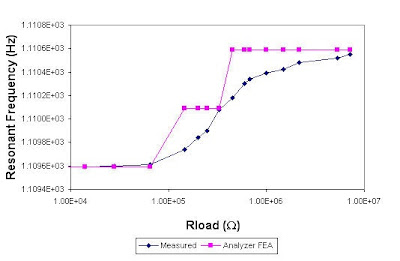
Figure 3 and Figure 4 compare measured and simulated values for average power dissipated and resonant frequency with load resistance, respectively. The measured data accuracy is estimated to be 6%. Predicted power dissipation is within about 25% of the nominal measured values, mesh refinement on selected simulations suggest a reduction to 21% is possible. The remaining difference is likely due to slightly high material damping values used for simulation. Figure 5 shows an animation of harmonic displacement magnitude together with the real voltage on the upper electrode.
Figure 3: Comparison of simulated and measured average power dissipated in a load resistor at 0.25 g acceleration. Note the measured point at Rload of 7.1 Mohm is likely erroneous.
Figure 4: Comparison of simulated and measured shift in resonance frequency at 0.25 g acceleration. The step in the simulated data is due to the 0.25 Hz frequency increment of the harmonic analysis


Figure 5: Animation of harmnonic simulation showing displacement (scaled by a factor of 20) and real voltage developed on the upper piezo surface.

Nombre: Lenny D. Ramirez C.
Asignatura: CRF
Dirección: http://www.coventor.com/mems/applications/PZE_Energy_Harvester.html
Ver blogg: http://lennyramirez-crf3.blogspot.com/

Dual Mass Gyroscope


This dual mass gyroscope consists of two perforated proof masses supported by a system of suspension elements. Attached to the ends of each proof mass are interdigitated comb-finger capacitors. The comb capacitors are used for electrostatically driving the proof masses in anti-phase in a mode parallel to the substrate (the x direction). Rotation about the in-plane y-axis induces a Coriolis force, which deflects the proof masses in opposite directions, perpendicular to the substrate. Beneath the plates are deposited metal electrodes that are biased with a DC voltage. The proof mass motion in the z direction, resulting from the rotation of the gyroscope, induces current flow on the electrodes, which is then measured. Figure 1 shows the 3-D model of the gyroscope.

Figure 1: 3D model of the dual mass gyroscope. For clarity, the model has been scaled factor of 2 in the Z direction


Modeling:

In this example, Architect is employed to build a fully parametric, 3-D model of the gyroscope using plates, beams, electrodes and comb-finger elements from the Parameterized Electromechanical (PEM) parts library. Figure 2 shows the Architect schematic of the gyroscope.


Figure 2: Architect schematic of dual mass gyroscope

The perforated proof masses are modeled using components labeled "Rigid Plate". Similarly, the electrodes beneath the proof masses, which sense the proof mass motion, are modeled by components labeled "Electrode". The comb drives on either side of the two proof masses are modeled by "Straight Comb" components. The suspension elements for the proof masses are modeled using a combination of "Box-beam" and "Beam" components. Note that the Architect PEM parts library has a variety of beam-like suspensions structures, and a single "Box-Beam" element could therefore be used instead of using four rectangular "Straight" beams.
Simulation

Figure 3a shows the simulated displacement of the proof mass in the x and z direction over a period of 50ms. Figure 3b shows the first 5ms only. The simulation starts from the steady state, computed with a small signal AC analysis. The excitation voltages applied to the comb-drives vibrates the proof masses in the x direction at a frequency of 16.987 KHz. Angular velocity applied about y direction, after 1ms, induces a Coriolis force that causes proof mass motion in the z direction. This motion is sensed by measuring the difference in capacitance, "Delta Cap" in the output plot, between the two sensing electrodes. After 25ms the rotation rate about the y axis returns to zero, and the output signal decreases to a steady-state value. In this simulation modal (Rayleigh) damping models are used for the beam and velocity damping values used for the plate. The fully coupled electro-mechanical 50ms simulation takes about 1 hr to run on a 2 GHz processor.

Figure 3a: Gyroscope transient simulation showing input rotation about y, sense capacitance "delta cap", (right) mass displacement "x" and "z".


Figure 3b: Gyroscope transient simulation from (a) with response from 0 to 5.0ms.


Figure 4: Animation of transient simulation. For clarity, the fixed electrodes and the comb drives are transparent and the thickness scaled by 2. The displacement in Z is also scaled by a factor of 1,00,000 to allow the movement of the gyroscope to be resolved.


Nombre: Lenny D. Ramirez C.
Asignatura: CRF
Dirección: http://www.coventor.com/mems/applications/Dual_mass_gyroscope.html
Ver blogg: http://lennyramirez-crf3.blogspot.com/

Ring Gyroscope


This Ring Gyroscope is constructed from an outer ring, eight semicircular support springs, drive, sense and control electrodes, see Figure 1. The Gyroscope has two identical elliptically-shaped flexural-modes of that are of equal frequency and separated by a 45 degree angle, see Figure 2. The ring is excited electrostatically into the primary flexural mode, and held at a fixed amplitude. As device is subjected to rotation around its normal axis, Coriolis force causes energy to be transferred from the primary mode to the secondary mode, causing the secondary mode amplitude to increase. This amplitude change is sensed capacitively.


Figure 2: The first and second modes of the gyroscope. (a) first flexural mode, and (b) second flexural mode located 45 degrees apart from the first. Both modes have the same frequency.

Modeling:

Architect can be used to build a fully parametric 3D model of the Gyroscope using beams and electrodes from the Parameterized ElectroMechanical (PEM) parts library. Figure 3 shows the schematic of the Gyroscope. In the schematic, a sub-assembly has been used to represent the eight springs in the gyroscope. This makes it easier to construct and understand the schematic. Figure 3a shows the top level schematic while figure 3b shows the lower level hierarchical element. The semicircular support spring is modeled using a combination of 'Arc beam' and 'Beam' components from the PEM parts library.


Figure 3: Hierarchical Ring Gyroscope schematic in Architect, (a) top level schmatic  and (b) lower level hierarchical elements

Simulation:
Figure 4 shows the frequency response of the Gyroscope, generated via a small signal ac analysis. The frequency at which the Gyroscope has flexural modes is 27.085 KHz. The simulation time for this analysis is ~1 second on a 2 GHz laptop. Figure 5 shows an animation of the flexural mode shape at the resonant frequency, created using Scene3D.

Note that process variations can cause asymmetry in the ring structure which will lead to separation of the modes. Architect can help you understand the separation in resonances with process variation.
Figure 4: Small signal ac analysis result showing the displacement magnitude response at 27087 Hz


Figure 5: Animation showing first flexural mode. For clarity, the displacement is scaled up by a factor of 5000


Nombre: Lenny D. Ramirez C.
Asignatura: CRF
Dirección: http://www.coventor.com/mems/applications/Ring_gyroscope.html
Ver blogg: http://lennyramirez-crf3.blogspot.com/

MEMS Products Available in the Market


Freescale ZSTAR3: the multiple wireless sensing triple-axis reference design

The ZSTAR3 development tool contains one accelerometer transmitter boards and one USB receiver node. A ZSTAR3 system can accommodate upto 16 accelerometer transmitter boards, connected through an RF ZigBee 2.4GHz communication to a single USB node connected to a PC. The accelerometer boards measured acceleration in 3-axes using either a digital or analog sensor. The sensor sensitivity is defined by the selected accelerometer. The USB node is part of the ZSTAR and ZSTAR2 design, reprogrammed with dedicated SW supporting multiple nodes.


STMicroelectronics Unveils MEMS Digital Compass Module

STMicroelectronics (NYSE: STM), the leading supplier of MEMS for consumer and portable applications(1), has integrated a 3-axis digital accelerometer with a 3-axis digital magnetic sensor in a single module. The digital compass module combines high accuracy with small form factor and low power consumption at a competitive cost, meeting the growing market demand for advanced navigation capabilities and emerging smart location-based services. ST's high-performance system-in-package digital compass uses magneto-resistive technology from Honeywell and aims to accelerate the adoption of enhanced electronic compassing in portable consumer applications, including direction finding, map/display orientation, location-based services and pedestrian dead reckoning.


The LSM303DLH geomagnetic module combines magnetic-field and linear-acceleration sensing with an I²C digital interface in a single package, featuring six degrees of freedom (DoF).

The module offers:
- 3-axis acceleration sensor with user-selectable ±2 to ±8g full scale acceleration,
- a 3-axis magnetic sensor with user-selectable full scale (±1.3 to ±8.1 gauss).
The LSM303DLH includes, for each sensing element, an embedded self-test that can be performed before assembly, and smart power functionalities to minimize current consumption.
The module features two separate user-configurable interrupts for inertial wake-up and free-fall.


Epson Toyocom Develops the World's Smallest Single Package 6-Axis Sensor

Epson Toyocom Corporation, the leader in crystal devices, today announced the development of the AH-6100LR, the world's smallest* 6-axis sensor. This low-noise, low-power product comprises a 3-axis QMEMS*1 quartz gyro-sensor and an extremely stable 3-axis accelerometer within a single package.
Samples of the new AH-6100LR will become available in February 2010. Commercial development is scheduled for May 2010.


Colibrys New MEMS Accelerometer for Attitude Heading and Reference Systems (AHRS)

Colibrys (Switzerland) Ltd. has announced today the release of its new MS9005, a ±5g range MEMS accelerometer, to complement its existing family of +/-2g and +/-10g products targeted primarily at AHRS applications.

Current and future developers of AHRS using Colibrys accelerometers will benefit from this new product as an alternative to existing selection of products, which are the traditional Colibrys-MS9002 and MS9010 sensors dedicated to standard AHRS and the latest world's best open-loop RS9010 accelerometer dedicated to mid range requirements.

According to Jean-Michel Stauffer, VP Sales & Marketing at Colibrys, "the MS9005 offers optimal accelerometer performance for applications that operate in medium level vibration and shock environment but where absolute bias and scale factor stability and reduced VRE (Vibration Rectification Error) are valued. Typical examples of AHRS integrating Colibrys accelerometers are airplanes, helicopters and UAV as well as backup systems on large aircrafts and small jets. This new product strengthens Colibrys' position as the world leading supplier of MEMS accelerometers for AHRS applications"

his product benefits from the specialised knowledge and applications experience of Colibrys accelerometers in term of reliability for harsh environments and safety critical applications.


Nombre: Lenny D. Ramirez C.
Asignatura: CRF
Dirección: http://info.coventor.com/mems-products/
Ver blogg: http://lennyramirez-crf3.blogspot.com/

MEMS resonator: Thermo-Elastic Damping and Anchor Loss models


Resonator Design In CoventorWare

One of the design consideration for MEMS Resonators is the Quality Factor (Q). This is the ratio of the total stored energy to the energy dissipated in a single cycle. At a particular oscillation frequency, a higher Q indicates a lower rate of energy dissipation and oscillations die out more slowly.

Numerous physical loss mechanisms contribute to overall Q and can be expressed as:

QGAS

Air Damping: Squeeze film or Stokes
Minimized by operating in a vacuum
Coventor's Solution: Rayleigh Damping Coefficients

QTED

Thermoelastic Damping: As a vibrating body is strained, the temperature changes in proportion to the strain; when temperature gradients occur, heat conduction causes irreversible energy loss
Coventor's Solution: Thermoelastic Damping Option

QANCHOR

Anchor Loss: A fraction of elastic energy propagates into the surrounding support structure
Also referred to as support loss, clamping loss, or attachment loss
Coventor's Solution: QuietBoundary Surface Boundary Condition

QOTHER

Other Loss Mechanisms: Including structural dissipation (crystallographic defects) and surface effects
Coventor's Solution: Rayleigh Damping Coefficients
Thermoelastic Damping
The Thermoelastic Damping can contribute significantly to Q in MEMS resonators operating in vacuum. CoventorWare-ANALYZER's MemMech module calculates the energy lost to heat conduction caused by strain-induced temperature gradients. This direct harmonic analysis simulate in 32-bit mode and requires material properties such as thermal expansion coefficient (TCE Integral Form), thermal conductivity and specific Heat.

Temperature distribution during Thermo-Elastic Damping Simulation


TED Energy Distribution during Thermo-Elastic Damping Simulation


The graph below shows a comparison between a Thermo-Elastic Damping model that has been implemented in CoventorWare-ARCHITECT, Finite Element results from ANALYZER and analytical models.


Losses
Anchor losses result when anchors are stressed as a result of resonator displacement. A fraction of the vibration energy is lost from the resonator though elastic wave propagation into substrate. In MEMS structures we usually assume all elastic energy transferred to the substrate is lost, although the mechanism is not fully understood. Anchor losses can be significant if contributions from other loss mechanisms are negligible. Having a simulation tool provides the ability to investigate optimal anchor placement.
Acoustic waves propagate through the substrate causes energy loss at the anchor


The anchor loss can be calculated by modeling the resonator and a fictitious substrate, these are linked together in the simulation automatically (this avoids overly fine meshes). In addition a so called "QuietBoundary" boundary condition is applied which models elastic waves propagating to infinity in the substrate, eliminates the reflection of the elastic waves impinging on the boundary or excitation origin.

The results can be analyzed by plotting the harmonic displacement to identify the harmonic frequency closest to resonance. The Q factor and Harmonic Energy values can then be determined as can be seen in the result graph below:


Determining the Q factor from anchor loss calculations


Nombre: Lenny D. Ramirez C.
Asignatura: CRF
Dirección: http://info.coventor.com/memsahead/bid/34328/MEMS-resonator-Thermo-Elastic-Damping-and-Anchor-Loss-models
Ver blogg: http://lennyramirez-crf3.blogspot.com/

MEMS BUTTERFLY: Give your ideas wings with MEMS+ 2.0


Nature has inspired many designers to create new products that we use in our every day lives. The butterfly seems to be popular among scientists, see Qualcomm's iMOD display and others have designed gyroscopes.

Similarly, Coventor's product development created a test case inspired by the butterfly to demonstrate the new amazing capabilities of the MEMS model library that will be released in MEMS+ 2.0 in June this year.

The video above gives you a sneak preview of what's going to be possible with our upcoming MEMS+ 2.0 release.

Fastest computation of MEMS structures in Cadence Spectre

The video shows the first Eigenmode of a butterfly made of our new flexible plate components. The butterfly test structure was made of circular, quadrilateral and pie shaped flexible plates. Featuring 92 nodes, it was simulated in only 5 seconds with an AC analysis using Cadence Spectre. Constructing the model in MEMS+ 2.0 Innovator took less then 5min


AC simulation of the movement of butterfly wings using MEMS+ and Cadence Spectre

MEMS+ 2.0 user interface with access to foundry material and process data, 3D graphical interface for model creation and the MEMS model library.


Visualization of the connecting nodes of the 3D model. After creation of the 3D geometry the model can be simulated immediately in Cadence Spectre or UltraSim.


Nombre: Lenny D. Ramirez C.
Asignatura: CRF
Dirección: http://info.coventor.com/memsahead/bid/38416/MEMS-BUTTERFLY-Give-your-ideas-wings-with-MEMS-2-0
Ver blogg: http://lennyramirez-crf3.blogspot.com/

Dispositivos mecánicos ultra pequeños MEMS


Para fijar ideas podemos decir que en el microprocesador de una computadora actual tenemos unos 50 millones de transistores por cm2, lo que implica una dimensión típica de 1 m2 por transistor, con un detalle de los contornos del orden de los 100 nm. Esta miniaturización ha permitido reducir componentes electrónicos voluminosos dando a lugar a equipos portátiles, que de otra manera no se emplearían (radios personales, notebooks, teléfonos celulares, etc.) con un panorama de aplicaciones increíble.

¿Y qué tal si lográramos reducir máquinas enteras?

Se podrían construir, por ejemplo, pequeños dinamómetros (sensores de fuerza) que colocados en las patas de una cucaracha nos permitirían entender cómo efectúa y distribuye las fuerzas para lograr un desplazamiento tan eficiente en superficies no horizontales. Esta información nos llevaría eventualmente a construir nuevos dispositivos mecánicos en la escala humana para simular las técnicas de desplazamiento de estos insectos. También se podría armar, en dimensiones muy reducidas, un dispositivo ubicado en el cuerpo de un paciente ("lab on chip"), que analizara su sangre y que, en función de los resultados, inyectara fármacos en las dosis adecuadas, y hasta podría enviar una señal de alerta para que el paciente fuera atendido de urgencia. Estas máquinas funcionarían en definitiva como pequeños robots que nos permitirían la realización de un conjunto de tareas hasta hoy inaccesibles en un mundo de escala micrométrica.


La miniaturización de máquinas electromecánicas o MEMS ya es una realidad de nuestros días. Efectivamente, estos microdispositivos ya se emplean para la realización de acelerómetros, presentes en los airbags de los autos para determinar el momento justo en que se produce un choque y disparar así el mecanismo de inflado de las bolsas. Este mismo tipo de MEMS se emplean como elementos de navegación, particularmente en la industria aeroespacial, pero también se prevén aplicaciones como sensores de presión, temperatura y humedad. Se los ha incorporado en marcapasos, para sensar la actividad física del paciente y modificar su ritmo cardíaco. Para evitar falsificaciones de firmas, se ha pensado incorporar estos acelerómetros en lapiceras. De esta manera, no sólo estaría registrado el trazo particular de la firma sino también las velocidades y aceleraciones que le imprimió la mano a la lapicera mientras se firmaba, lo cual haría mucho más difícil su falsificación. También se emplean MEMS en los cabezales de las impresoras de chorro de tinta, produciendo la evaporación controlada de la tinta en el momento justo, y gracias a la entrega localizada de calor. Además de la ventaja del tamaño de estos dispositivos está el hecho de que se los puede fabricar de a miles abaratando notablemente su costo de fabricación.


Esquema del dispositivo que corrige las deformaciones de la imagen producidas por la turbulencia de la atmósfera terrestre. La óptica adaptable, realizada mediante MEMS, permite neutralizar este efecto y obtener una resolución angular adecuada como para distinguir objetos estelares que de otra manera se encontrarían confundidos en una imagen borrosa.
Nombre: Lenny D. Ramirez C.
Asignatura: CRF
Dirección: http://aportes.educ.ar/fisica/nucleo-teorico/estado-del-arte/nuevas-herramientas/dispositivos_mecanicos_ultra_p.php
Ver blogg: http://lennyramirez-crf3.blogspot.com/

MEMS Technological Developments


MEMS stands for Micro-Electro-Mechanical Systems and if that makes no sense to you, don't worry—lots of people are just discovering this new technology for themselves.

This unique system combines sensors, actuators, mechanical components, and electronics on one silicon base; essentially it is a type of glorified computer chip.
Typically, microfabrication is used to apply the various elements to their silicon wafer.

The many components that go on the wafer all have their different manufacturing processes: electronics are typically made separately using integrated circuit, or IC, process sequences (this can include BICMOS, CMOS, or Bipolar techniques.) The micromechanical elements, on the other hand, are often micromachined.

This means that a high-tech device, sometimes a laser cutter, etches away parts of the silicon chip, or sometimes areas are added in order to create the end result.With the advent of MEMS technology, the techno-geek dream of having an entire system on one chip has become reality.
Prior to MEMS, two separate components were required to work in tandem: the microelectronics on a silicon chip, and the micromachined mechanical elements in a different format. Combining them into one efficient MEMS system eliminates several steps of production as well as the need for a connector between the two elements.


This allows for the development of "smart" products because microelectronics can perform delicate computational functions which are then enacted by the fine-tuned physical accuracy of microsensors and microactuators. Smart MEMS products with these kinds of capabilities open up a whole new world of applications and technological design possibilities.

Understanding what the different parts of a MEMS chip are all about becomes easy when you think of the microelectronic integrated circuits as the brains of the operation, sending signals to the microsystems that will then act as eyes, arms, legs, etc. to carry out the desired action.

Once the microsensors have received the circuits' directions they sense their environment, measuring different factors such as thermal readings, biological presence, mechanical functions, chemicals, optical information, and magnetics—this information is then relayed back to the "brain" for more decision-making, and all of these steps take place in a matter of seconds.

The fact that MEMS microchips can to some degree make their own decisions fits in with other innovations in the field of nanotechnology; nanotech scientists have always made it plain that they are working toward an ideal autonomous product (which will perhaps reach its peak expression in the nanorobot, but is nevertheless an integral part of most nanotechnology products.

Decision-making capabilities as well as sensors that allow the MEMS chip to detect its environment are key factors in its superior functioning. The actuators usually perform functions like physically moving their entity, positioning in small increments, regulating data, pumping fluids or air, and filtering various substances.

Typically the functions associated with a device that uses MEMS technology are somehow related to controlling the surrounding environment in order to achieve a desired outcome. Before MEMS technology other devices were capable of doing similar tasks, but to date none has been as efficient as MEMS.

This is because MEMS chips can typically be made using batch fabrication manufacturing in much the same way that integrated circuits are produced, which renders them extremely low in cost as well as more functional, more reliable, and also more sophisticated. And perhaps the best part is that all of these superior features can be combined onto one small silicon chip.

Almost every industry can benefit from having such fine-tuned technology at their disposal. The dual nature of MEMS systems allow them to bridge gaps between previously unassociated subjects, such as microelectronics and biology, for example.

Biotechnology has benefited from MEMS developments like the Polymerase Chain Reaction microsystems which can be used to amplify and identify DNA. MEMS has also given rise to Scanning Tunneling Microscopes, which are made with the micromachining process; biochips that have the ability to scan and detect chemical and biological agents which may be hazardous; and microsystems that render drug screening and selection more effective.
In the communications field, high frequency circuits have been upgraded with MEMS technology so that they can perform better and more cost-efficiently. Electrical elements of these circuits tend to benefit the most, such as their tunable capacitors and their inductors—and best of all, production and installation become a simplified process because no integration is required when MEMS is used.

The mechanical switches used to run these systems also show large improvements when upgraded with MEMS. The only drawback for MEMS communications devices lies in their reliability and packaging; in some cases the same product has had consistency issues across the board and resolving these problems will prompt greater acceptance in the marketplace.

Accelerometers are used for a variety of scientific applications, and MEMS can improve these functions too. MEMS accelerometers are quickly rendering their conventional counterparts obsolete, especially when it comes to airbag deployment in automobiles

MEMS accelerometers can sense not only the fact that an impact has occurred, but they can also judge the speed, intensity, and several other crash-related factors in order to determine the rate at which an airbag system should deploy and also how much of the airbag to release.

This has the potential to save lives, since too much or too little airbag has often resulted in crash deaths. The traditional accelerometer is actually a series of devices integrated together at various points throughout the vehicle, with their attendant electronics positioned near the airbag.

This system is not only clunky and awkward, but allows the system parts to become cut off from each other at several points, possibly resulting in complete lack of accuracy or even a total system malfunction.

This conventional accelerometer package typically costs about $50 per vehicle. MEMS nanotech accelerometers, on the other hand, can integrate all the fundamental parts onto one small silicon chip. Such an approach renders them lighter, more accurate, and less expensive—MEMS accelerometers tend to average about $5 or $10 per vehicle, saving the consumer money many times over.

Nombre: Lenny D. Ramirez C.
Asignatura: CRF
Dirección: http://nanogloss.com/mems/mems-technological-developments/
Ver blogg: http://lennyramirez-crf3.blogspot.com/